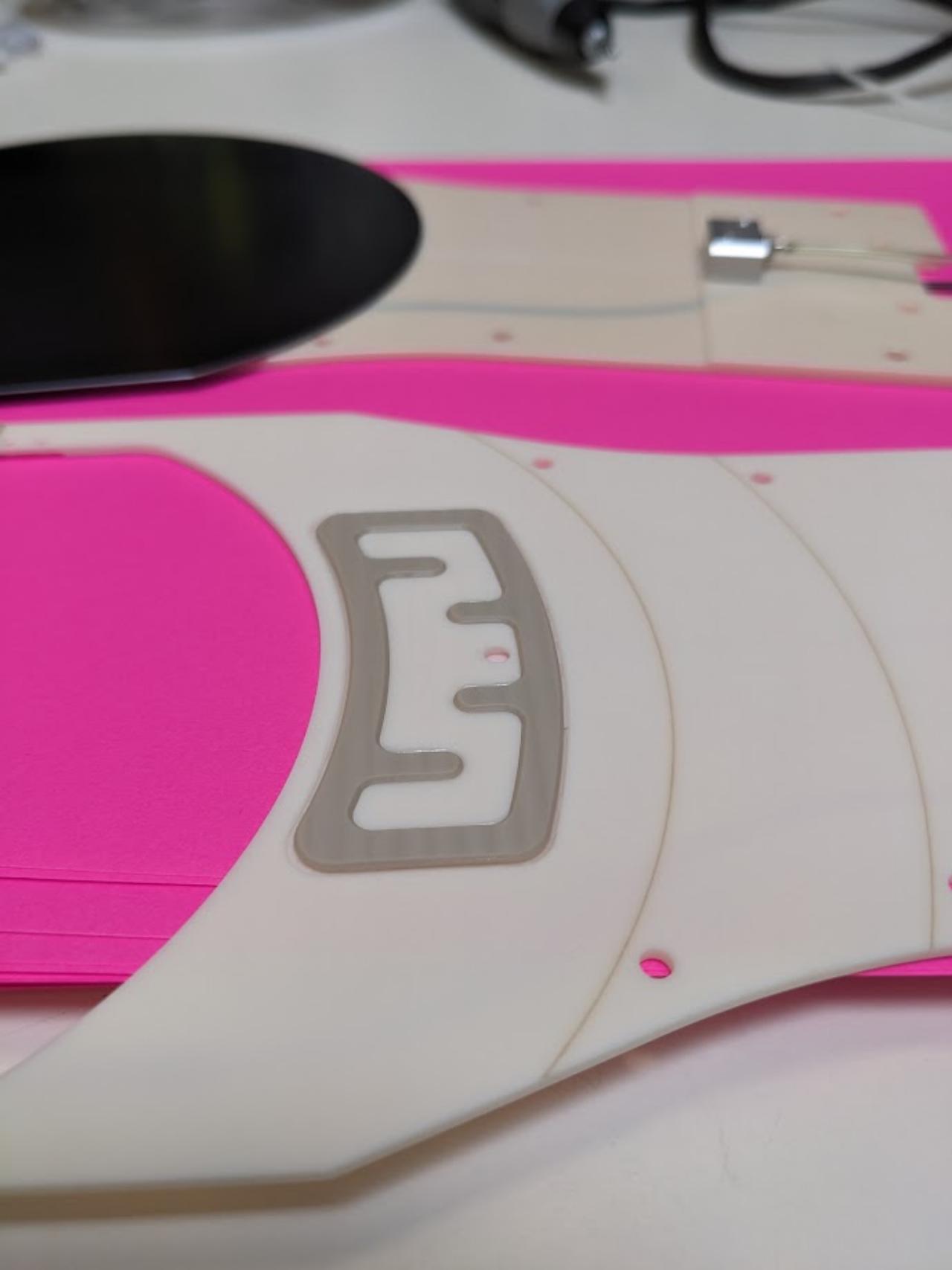
Customer reported wafer slip issues with an older design, due to the offset vacuum pad. This updated vacuum pad with increased vacuum surface area fixed the issue.
A robot with thin dual edge grip end effectors. This is used to handle 200mm diameter wafers that are stacked 6.35mm apart. Many thin end effector applications require ceramic material for the rigidity, which has its own design considerations to account for.
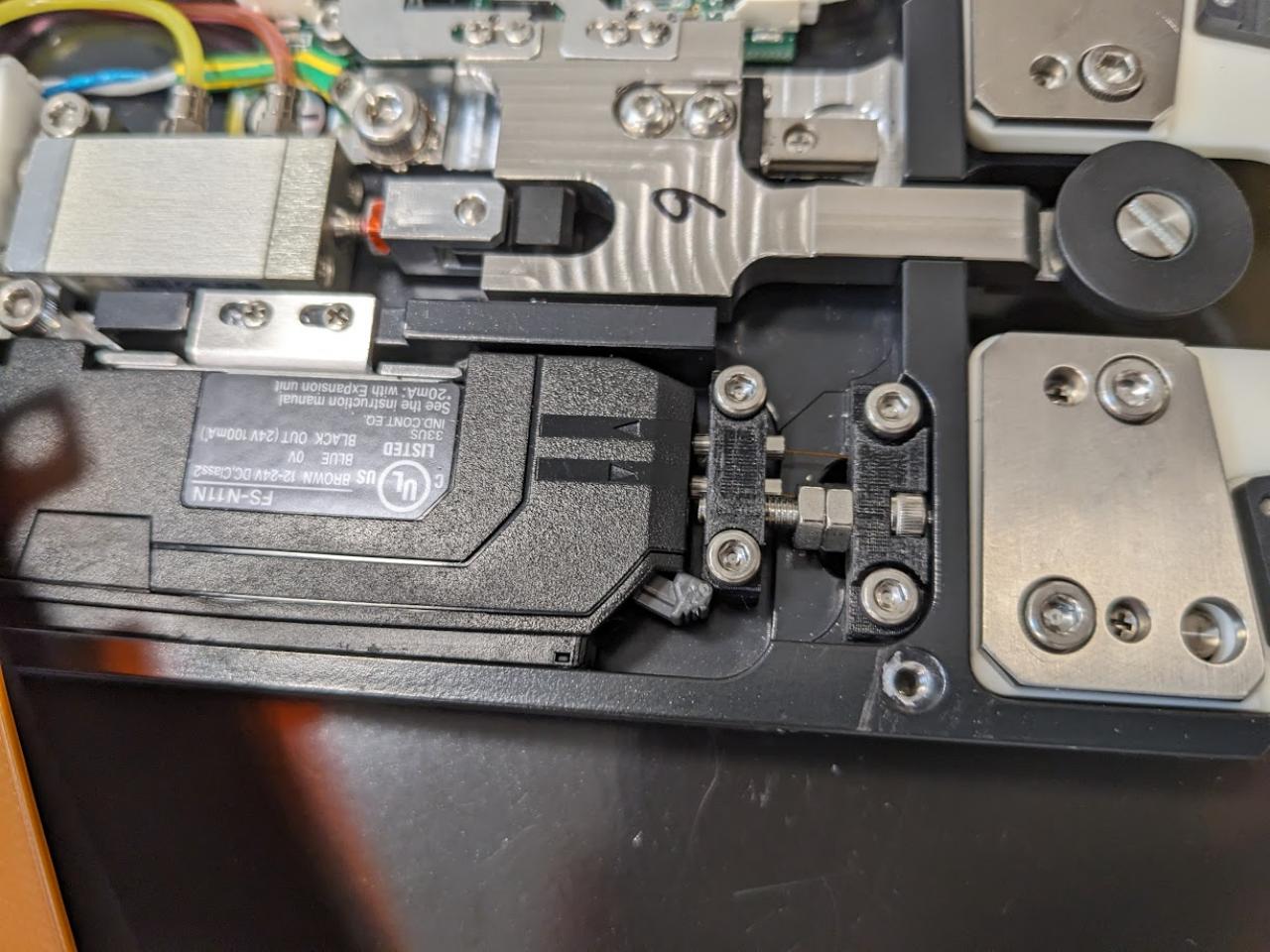
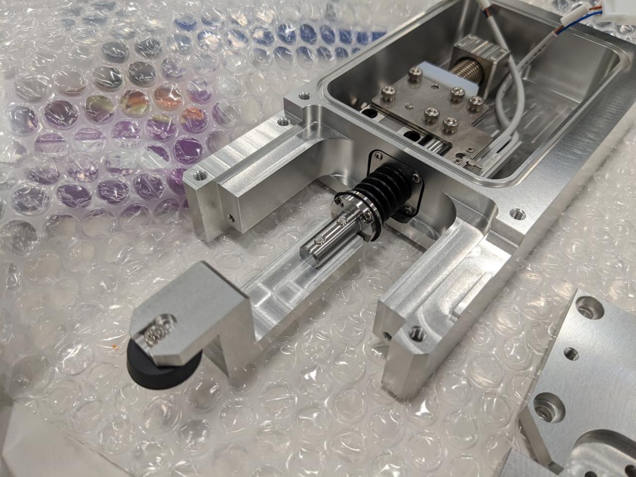
When charting the characteristics of a new mapping sensor, we needed a way to fine tune the light intensity reading into the mapping amplifier. Previous methods involved adjusting the port depth by hand, which was very coarse. I designed a mapping fiber adjustment jig to pull the port out of the mapping ampilifer at a controlled pace, allowing me to finish my analysis of the mapping sensor.
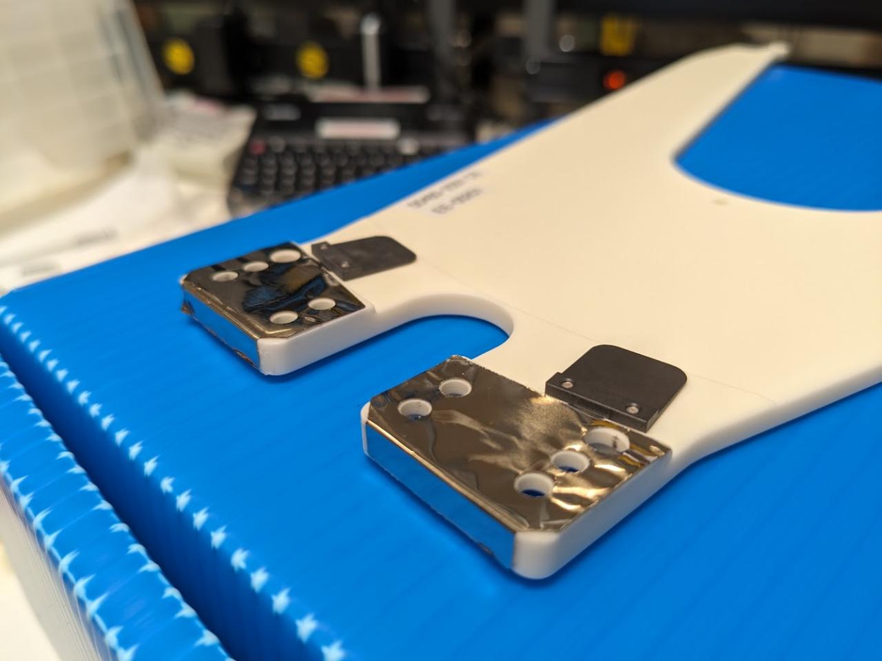
Grounding shims for a rush order. Traditionally for ceramic end effectors, the ESD path from wafer to ground is transferred thru the end effector using an ESD coating, since ceramic is an insulator. However, a customer requested an ESD capatible-end effector much earlier than the ceramic lead time, and the only ceramic end effector available was an uncoated one. I ideated and designed thin grounding shims underneath the wafer guides to bridge the ESD path, and we managed to get the ESD end effector to the customer on time.
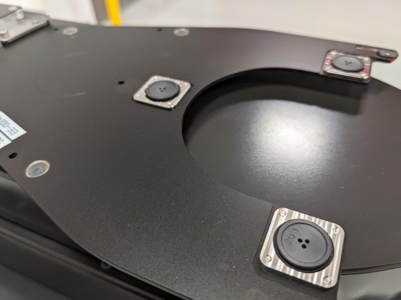
Traditional robots handled flat wafers, but more requests are coming in for the handling of warped wafers. To handle both umbrella bow and bowl bow warped wafers, we designed a pivot pad vacuum end effector with different replaceable pivot pads for different bow amounts. The pivot pad height is determined by the bow amount, but also the pitch between wafers in the FOUP, deflection due to payload mass, vibration spec and more.
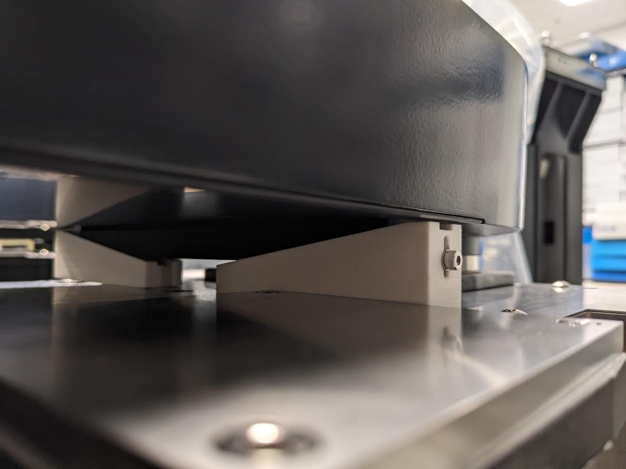
To prevent a SCARA type Z-arm from vibrating down past software limits during transit, a solid plastic block is placed below the lower arm. However, after transit at the customer site, these are very difficult to remove without first powering on the robot and moving the Z-arm up, which is sometimes not possible. To solve this, I designed a prototype wedged shipping block that allows for uninstallation without robot power, just loosen the screws and the white wedges will slide off the middle black wedge.
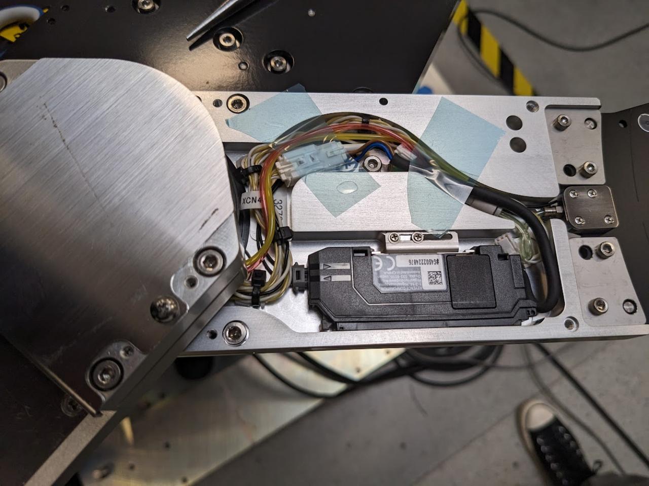
A new customer request came in to handle extra-heavy payloads on both hands of a dual hand robot. Existing dual hand robots have extra-heavy payload capabilities, but only on the upper hand. This new lower hand was designed in NX, tested in ANSYS to match the deflection of the existing upper hand. Special consideration was given to the fiber routing and the existing harness lengths.
In a wet environment, great care is taken to ensure moisture does not enter the robot internals. For a linear actuating plunger, I designed both the rubber bellows and the testing jig made for lifetime reliaiblity testing, which is what is shown here. The lifetime reliability testing is done under the most rigorous conditions, completely underwater for one year. The white strip on the shaft is moisture detection paper.